


What is the current state of microscale 3D printing?
Microfabrication is the process of fabricating miniature structures of micrometer scales and smaller. Historically, microfabrication was first used in the electronics industry to miniaturize the size of devices. In fact, over the years, you might have noticed your electronic devices have been getting smaller and sleeker. Component sizes that were in tens of micrometers became single-digit micrometers, and then hundreds of nanometers, and then went down to a few tens of nanometers, where they stand today. As a result, what used to be called microfabrication was rebranded as nanofabrication, although the governing principles have remained essentially the same. To meet the challenge of shrinking component size in the electronics industry, new tools and techniques are continuously being developed. One of these techniques is microscale 3D printing. So what applications are enabled by microscale additive manufacturing? And more generally what are the benefits of micro 3D printing?
First of all, we should note that in the world of additive manufacturing, the electronics industry is one of the least well versed in the technology. If we consider that aerospace was one of the first sectors to adopt and develop 3D printing, electronics is essentially the opposite. Nevertheless, additive manufacturing can bring benefits and new capabilities to this sector by enabling a new-level of customization for micro and nanoscale components.
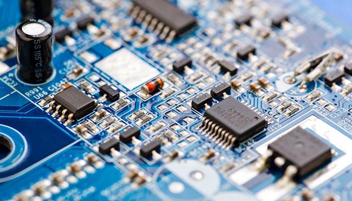
To meet the continuing challenge of shrinking component size in microelectronics, new tools and techniques are continuously being developed. The main driver of this technology being integrated circuits, such as the one above.
Indeed, microscale additive manufacturing was first developed to benefit the electronics industry, but today the technology is moving beyond this field. For example, the technique could be used for medical applications, where nano-sized components could enter the body to cure diseases, or for micro-optical elements. In the following piece, we look at multiple angles of the relationship between additive manufacturing and micro/nano fabrication to give you an overview of the current state of this technology and its applications in and beyond the electronics sectors.
The Technology Behind Microscale 3D Printing
Firstly, let’s consider the main technology behind microscale 3D printing, also known as microstereolithography. Microstereolithography is based on a manufacturing principle very similar to the one of stereolithography (SLA) – the first 3D printing technology to have been patented – but implements process improvements that result in a far better resolution (up to a couple of micrometers). It relies on the polymerization of a photosensitive material by ultraviolet light.
In the electronics segment, the technology needs to be capable of creating structures that are conductive and insulating at the same time, which is quite the challenge. Nano Dimension, one of the leading manufacturers of 3D printed electronic components, has introduced an inkjet 3D printing technology that uses nanoinks. Also based on photopolymerization, a printhead deposits dielectric nanoparticles, conductive nanoparticles and polymers onto the build plate, which are cured by UV light in between successive depositions. On the other hand, Optomec, another leading company in 3D printed electronics has developed Aerosol Jet 3D printing, which works by deposition of a tight stream of electronic inks as small as 10 µm.
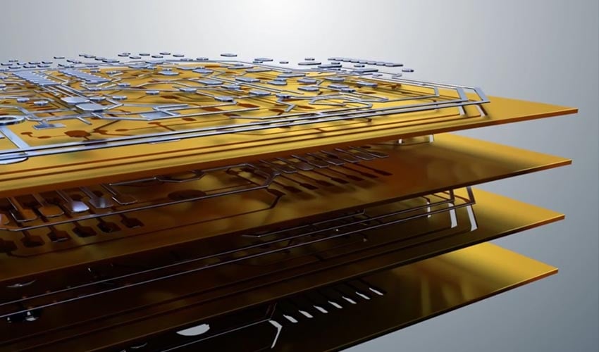
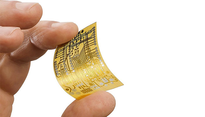
There is a great demand for printed circuit boards (PCBs) to become denser and more complex. The following PCB is multi-layer which means it contains multiple layers of conductive traces instead of containing only 1 | Credits: Nano Dimension
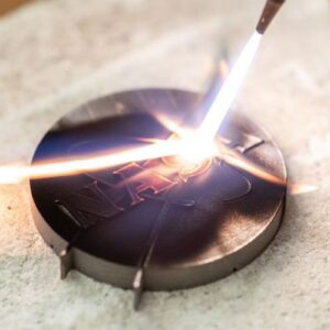
When it comes to metals, microstereolithography is no longer suitable. Micro laser sintering is a technology similar to Selective Laser Sintering (SLS) that has been developed to create metal 3D printed micro structures, and is used by actors such as 3D MicroPrint, based in Germany. Exaddon, on the other hand, relies on a process that could be compared to Directed Energy Deposition (DED), which they call electrochemical deposition. A micro-sized nozzle deposits a liquid of metal ions, which is transformed by an electrolytic process (electric charge) into solid atoms.
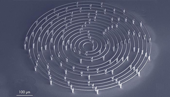
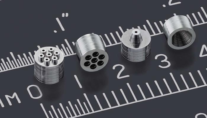
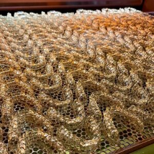
Manufacturing coils with a diameter less than 300 micrometers is a complex challenge which is hardly addressed by conventional methods. The following copper coils have been 3D printed by Exaddon in collaboration with Harvard Medical School | Credits: Exaddon
As for nanoscale 3D printing, the technology is called multiphoton lithography (MPL), most commonly known as two-photon polymerization (2PP). It uses, as its name suggests, the two-photon absorption of high intensity lasers such as near infrared light (NIR). These high-intensity lasers can create resolutions of up to 50 nm (0.05 µm). These parts being so tiny, they actually take more time to create than one might first expect. This process is lengthy because it polymerizes such small areas at a time, and for this reason it is difficult to scale up. To give you an idea, the naked eye can see objects as small as 0.1 mm, so about 100 micrometers (µm). Therefore, you would be unable to see many of the structures that two photon polymerization (2PP) is capable of creating.
In fact, researchers in multiple universities around the world are studying the capabilities of 2PP. Recently, at the Chinese University of Hong Kong (CUHK), in collaboration with Lawrence Livermore National Laboratory, researchers have been working on improving 2PP. Sourabh Saha, leader of this research project, explains: “Traditionally, there are tradeoffs between speed and resolution. If you want a faster process, you lose in resolution. We have broken this engineering tradeoff, allowing us to print a thousand times faster with the smallest of features.” Essentially, the researchers are replacing the singular high intensity laser with a field of light to accelerate the process.
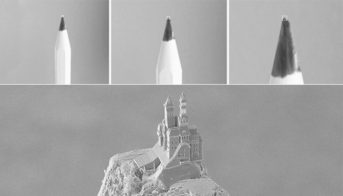
This castle measures 230 µm x 250 µm x 360 µm, and has been 3D printed on top of a pencil using 2PP | Credits: TU Wien
The Applications of Microscale 3D Printing
Electronics Industry
As mentioned, in the electronics field, micro 3D printing can improve performance, functionality and increase the miniaturization of devices. For engineers, one of the challenges of innovating in this field is often creating prototypes to test the shape or the embedding of the electronics in order to authenticate new product designs. By prototyping in-house instead of outsourcing, manufacturers can benefit from shorter lead times, design flexibility, customization and a simplified supply chain. Micro 3D printing can be used to create new designs for devices such as embedded electronics, electromagnets, MIDS (Molded Interconnect Devices), antennas, sensors and multi-layer PCBs (Printed Circuit Boards).
The CEO of Nano Dimension, Amit Dror explains that many sectors will benefit from this technology beyond prototyping applications: “Today, the stronger need for AME (additive manufacturing electronics) solutions arrives from aerospace and defense industries, where the need for high-mix low-volume parts is clear. Looking to the horizon we can expect industrial scale production coming from the automotive industry and from the electronics consumer goods.”
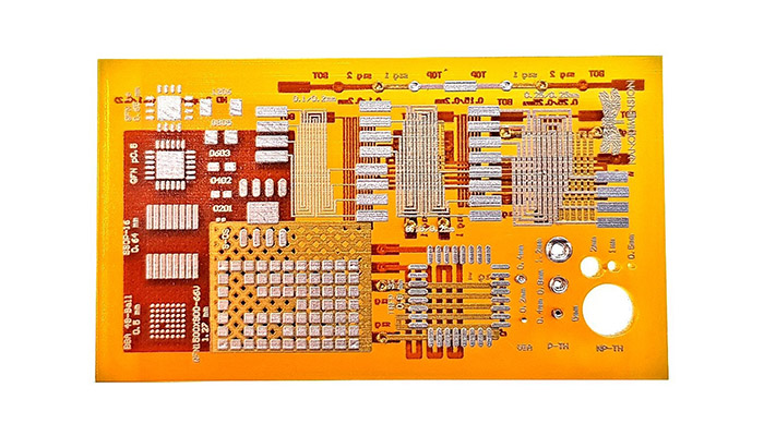
Nano Dimension’s precision 3D printed PCB prototype produced on the DragonFly Pro | Credits: Nano Dimension
3D printing electronics has a high chance of following the same path as early adopters of the technology. As the technology matures and new players enter the market, 3D printing of electronics could eventually shift from being solely a prototyping tool to a mass production process. To give you an idea, Optomec, the other leading company in this segment of additive manufacturing explains that its Aerosol Jet technology is capable of 3D printing 5,000 integrated circuits sized 25 to 50 µm per hour, and production can be scaled up to 10,000 per hour with the introduction of an additional nozzle. In other words, the company already promises that its technology is scalable to support high-volume production.
Other Applications
Of course, there are other fallout benefits of being able to print such small structures. Multiple startups like Microfabrica, Nanoscribe, Boston Micro Fabrication or MicroLight3D have developed micro technologies that can be used to produce medical devices. For medical professionals, minimizing the amount of collateral tissue damage during an operation is a priority. Therefore, miniaturizing medical devices is key. Still in the medical sector, Nanoscribe explains that users can fabricate 3D scaffolds to study cell growth, migration or stem cell differentiation on biomimetic structures using its 2PP technology. The startup also uses 2PP for a range of other applications such as refractive, diffractive and micro optics.
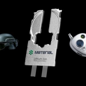
3D printed tools showcasing micrometer precision using metal micro 3D printing | Credits: Microfabrica
What does the future hold for this segment of AM?
In the future, possible applications include producing wearable or embedded sensors for real-time health monitoring. Additionally, 3D printed sensors could be built into lenses to enable augmented reality applications, whilst 3D printed embedded electronics could be seen in objects from smartphones to cars, adding functionality whilst making them lighter. The limitations today concern the software to develop the models for such small manufacturing, but also expanding the materials available for this process.
To conclude, it’s pretty evident that the wider adoption of micro 3D printing will meet the same hurdles as other additive manufacturing technologies. John Kawola, CEO of Boston Micro Fabrication told us: “We don’t believe the challenges of wider adoption of microscale 3D printing are any different from the challenges of wider adoption of 3D printing in general. 3D printing across all sizes will continue to be valuable for engineering and design prototyping. Microscale 3D printing brings some new tools to the engineers who previously couldn’t effectively prototype at that scale. In addition, the production of microscale parts are typically quite expensive, thus increasing the value of considering 3D printing for production of end use parts.”
What do you think microscale 3D printing will bring to the additive manufacturing industry? Let us know in a comment below or on our Facebook and Twitter pages! Don’t forget to sign up for our free weekly Newsletter, with all the latest news in 3D printing delivered straight to your inbox!


Hey,
My name Is Boaz I am intersted of the technlogy of the nano bible do you know about this product?
The Nano Bible is a gold-plated silicon chip the size of a pinhead on which the entire Hebrew Bible is engraved. The text, consisting of over 1.2 million letters, is carved on the 0.5mm2 chip by means of a focused ion beam.
Hello Boaz, It is possible to create such product using e.g. electron beam lithography. If you are still interested, please let me know. ma**********@******up.cz