University Researchers Create New Method to Print Copper on Fabric for Wearable Electronics
Recently, researchers from the Department of Electrical Engineering at the University of South Florida (USF) received a patent and official grant of $369,574 from the National Science Foundation (NSF). This will be used for the development of a method to 3D print copper directly on fabric. The new electrochemical process marks a new milestone in the advancement of wearable electronics.
In this day and age, electronic gadgets have developed to a level that no one would have imagined a few decades ago. Long gone are the days of chunky devices that served a single purpose only. Nowadays we have smartwatches, multifunctional headphones, and even wearable computer glasses are available, and it is not inconceivable that the possibility of having wearable electronics that are embedded into clothing might be just around the corner. In an attempt to further advance such technologies, Department of Electrical Engineering Associate Professor Arash Takshi and USF Research & Innovation Interim Vice President and Professor Sylvia Thomas have developed a new method called hydrogen evolution assisted (HEA) electroplating that makes it possible to print copper directly on fabrics, opening the door to an abundance of technological innovations.
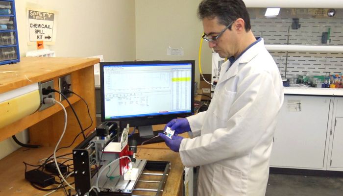
Professor Arash Takshi at Work (photo credits: USF)
Creating Wearable Electronics with Copper 3D Printing
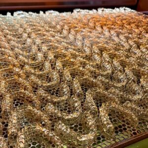
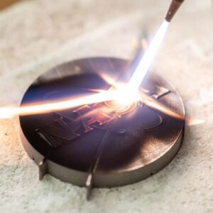
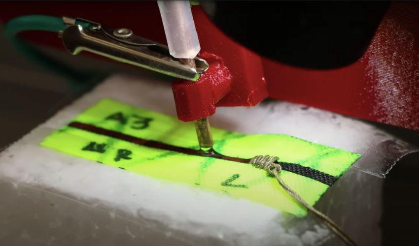
The new process consists of two steps of additive manufacturing. First, laser printing technology is used to apply a conductive template to the fabric. In the process, the fabric is carbonized, which enhances its stability and makes it more durable. In the next step, electroplate copper is used to produce a continuous copper pattern that forms the circuit layout of the electronic component on the fabric. The specially designed nozzle, that is mounted on a 3D printing device, enables localized electroplating and makes it possible to make the copper grow in the junctions between the electronic components’ terminals and the circuit printed layout, and solder them at room temperature. The main difference between the newly introduced method and the way it has been done in the past is that Takshi and Thomas’ method increased the voltage applied during the process, which ultimately results in the water electrolysis at the same time that copper grows, making the process faster and enhancing the mechanical stability of the printed structure.
Professor Arash Takshi explains, “The current technology for wearable electronics is mainly based on printing conductive inks consisting of nanoparticles of metals and/or carbon. The process relies on the physical connections of nanoparticles after drying the pattern. However, the high electric resistance from a conductive path made of conductive nanoparticles limits the applications to simple wearable electronic designs. These aren’t suitable for sensitive measurements and high electric current applications.” Thanks to this two-step additive manufacturing method, it would be possible to create these longer-lasting wearable technologies without damaging the fabrics as it is often the case when using methods like soldering.
With the recently received patent and the financial boost from the NSF, the promising new method could be further developed and may soon be used in future projects in different sectors such as the health, military, or even aerospace. For example, soldiers could wear new smart suits that aid them in combat, or astronauts could have suits that benefit them on space missions. The technology could even be used to monitor patients’ health status. Indeed, the researchers seem sure that the technology, although still requiring many hours of research and development until it can be used, is very likely to someday make our lives easier in many ways thanks to more easily achieved wearable electronics. You can read more about it in the press release HERE.
What do you think of this new method? Let us know in a comment below or on our LinkedIn, Facebook, and Twitter pages! Don’t forget to sign up for our free weekly Newsletter here, the latest 3D printing news straight to your inbox! You can also find all our videos on our YouTube channel.
*Cover Photo Credits: USF