UT Austin Unveils New 3D Printing Method for Advanced Electronics

A research team led by The University of Texas at Austin has introduced a new 3D printing technique that could redefine how semiconductor components are designed and produced. The method, known as Holographic Metasurface Nano-Lithography (HMNL), offers a way to print chip packages and electronic structures at speeds and levels of complexity that traditional manufacturing cannot match.
Semiconductor fabrication is typically slow and expensive, relying on a long sequence of material deposition, masking, etching, and packaging steps. Each stage increases cost, limits design flexibility, and produces waste. HMNL replaces much of this workflow with a single 3D printing process that patterns advanced electronics in one pass. The technology can fabricate multi-material, three-dimensional structures that integrate metals and polymers in highly detailed geometries.
An example of the Holographic Metasurface Nano-Lithography (HMNL) method on a semiconductor.
At the center of the process are metasurfaces, ultra-thin optical masks that contain dense patterns of encoded information. When illuminated, these surfaces project holograms into a hybrid resin that solidifies into precise microstructures. Researchers say HMNL can reach features smaller than a human hair and can create forms that are impossible to achieve with step-by-step lithography. This opens the door to new component categories such as fully 3D printed capacitors, non-planar chip packages, and electronics shaped to fit robotics or aerospace systems where space is limited.
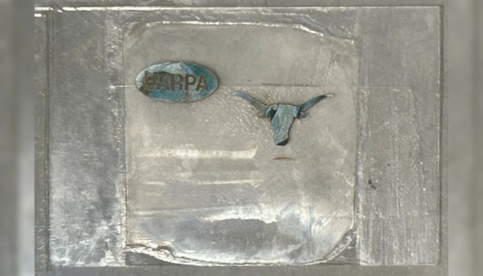
The project, supported by a 14.5 million USD award from DARPA, includes partners across both academia and industry. Researchers from the University of Utah, Applied Materials, Electroninks, NXP Semiconductors, Northrop Grumman, Bright Silicon Technologies and Texas Microsintering are working together to accelerate the development and testing of HMNL-based electronics.

Research continues to be spearheaded by the Cockrell School of Engineering at the University of Texas at Austin.
Early prototypes demonstrate the range of applications. One example is a fan-out module created for consumer devices, while another prototype focuses on high-frequency systems for defense. The team has also printed electronics that wrap around curved surfaces and active packages that combine mechanical strength with electrical functionality. These designs show how 3D printed microscale structures could support rapid prototyping and lower environmental impact by cutting material waste and simplifying supply chains.
The project’s commercial path runs through Texas Microsintering Inc., a startup founded to bring HMNL to market. The company plans to scale the technique so that chip designers can produce custom electronic packages in days instead of months.
With semiconductor manufacturing under pressure to increase efficiency while supporting more powerful devices, HMNL offers a potential shift in how the industry approaches the most fundamental parts of the chipmaking process. By merging advanced optics with 3D printing, the research team is positioning additive manufacturing as a viable tool for future electronics production.
What are your thoughts on UT Austin’s developments? Let us know in a comment below or on our LinkedIn or Facebook pages! Plus, don’t forget to sign up for our free weekly Newsletter to get the latest 3D printing news straight to your inbox. You can also find all our videos on our YouTube channel.
*All Photo Credits: University of Texas at Austin