#3Dstartup: Voltera designs printed circuit boards thanks to additive manufacturing
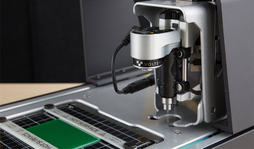
Less often discussed, additive manufacturing also has its place in the electronics sector, where it enables the design of smaller, finer and more precise components than conventional production methods. Known as micro 3D printing, this technique can improve the performance, functionality and miniaturisation of devices. It is often used in prototyping stages before the final product is manufactured. In fact, the startup we interview today, called Voltera, is interested in additive manufacturing to design printed circuits, beyond prototyping. Voltera has developed a machine to create its own circuits, hoping to revolutionise the electronics sector by making this 3D printing technology more accessible. We met with Alroy Almeida, one of the founders of the company, to learn more about the functionalities of its 3D printer and his vision of the sector!
3DN: Can you present yourself and tell us about your relationship with 3D printing?
I’m Alroy from Voltera. My background with 3D printing goes back 10 years, creating mechanical components for projects. At Voltera we do a fair amount of prototyping – originally with a filament-based printer but over the last few years we’ve moved to SLA (on our own machine and through print shops). While I still keep on top of what’s happening in the 3D printing space, since Voltera is an Additive Electronics company, I’m incredibly intrigued about the current state of the art and future developments of AE technologies.
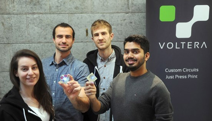
Part of the Voltera team, Alroy is at the right
3DN: Why did you decide to launch Voltera?
In 2012 we realized that 3D printers were very handy for mechanical prototyping but a circuit printer didn’t exist for electronics engineers. During the early stages of product development, it is awful to wait weeks for prototypes to arrive from factories or to pay ridiculous fees to expedite delivery. The electronics were becoming the bottlenecks at many companies. We learned this the hard way while designing electronics at various companies. Personally, my background was in industrial electronics (ruggedized communications for factories and other harsh environments) but I also did some development on medical devices. My business partners had plenty of experience in automation, EDS, and materials research.
We decided to put our Mechatronics and Nanotechnology Engineering degrees to good use by creating a circuit printer. At first, it was to scratch our own itch… just to see if we could do it. However, pretty soon we started getting interested from former colleagues and friends so we decided to take it from a project to a product.
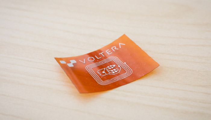
A 3D printed circuit by Voltera
3DN: Can you tell us how the V-one printer works?
Before we talk about the machine prints circuits it is worth discussing how the circuit gets designed in the first place. Our CAM software accepts Gerber files (the standard PCB layout format) which can be exported from whatever CAD tool you are already using – we’re completely agnostic to the CAD tool and don’t want to disrupt your existing design process. Once you open the Gerber files in our software converts the input files into tool paths, the machine calibrates, and it is ready to begin creating the board.
The steps the machine goes through for creating a double-sided board are:
1) drilling holes for vias and through-hole components
2) printing the top layer of the circuit and then thermally curing it
3) printing the bottom layer of the circuit and then thermally curing it
4) PCB rivets for vias are quickly added manually
5) dispensing solder paste onto pads
6) components are added manually and then are reflowed into place by the machine
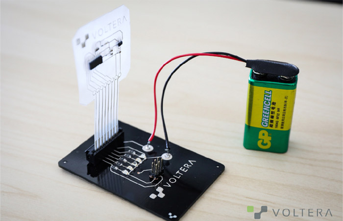
The full spec for the printer can be found here but the highlights are double-sided circuits with 0.65mm pin-to-pin pitch, passives down to 0402, 8mil space and trace, and a 128mm × 116mm print area. The machine comes in European and North American plugs and voltages. The conductive ink used to create the traces is silver-based but this doesn’t mean that it is expensive. In fact, each $99 ink cartridge can print dozens of boards and each $49 cartridge of solder paste can cover thousands of pads. The standard substrates you can print on are FR4 and FR1 fiberglass boards however many users print on glass, paper, PI, PET, and others. The 550W heater in the machine thermally cures the ink and reflows the solder paste using standard and custom heating profiles.
3DN: What is your company’s mission?
We currently have thousands of V-One machines in over 65 countries around the world. They are being used by hardware businesses of all sizes to bring new ideas to market faster, academic and government researchers for breakthrough technologies, and educators in high schools, colleges, and universities to train the engineers of the future. These machines are being used to develop robots, satellites, medical technologies, automotive components, and dozens of other applications.
Our current goal is to continue empowering our customers and to help new users build hardware faster. Especially now in 2020 when so many businesses have lost time and resources to the pandemic, hardware developers are being asked to do more with less. They are being asked to hit deadlines despite working from home.
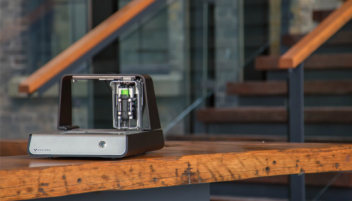
Thanks to its size, the Voltera machine is adapted to all types of environments
The V-One was designed to sit on your workbench but it is small enough to feel at home on your dining table or home office. Hardware development processes are already shifting and you now have the ability to email design files to a colleague across the city or planet and have them print a board in an hour. No more waiting for factories or shipping parts back and forth. We’ve had customers who were working on respirators and COVID-19 testing devices that were able to get through development so much faster because they had a mini PCB factory on their desk.
3DN: What are the future projects of Voltera? Where do you see the company in 5 years?
While the majority of V-Ones are being used by businesses, we see a huge opportunity to work with more educators. The machine was designed for professionals but is so easy to use that it is being used by university and high school students around the world. We see it playing a huge part in hands-on electronics education. While the theory and math behind electronics is important, it is the hands-on creative component that will inspire students to pursue careers in product development.
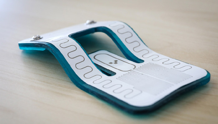
Our product roadmap is highly influenced by our users and the machines we currently have in development are a direct response to them hacking the V-One to create more exotic forms of electronics – circuits that can flex or stretch, circuits that conform to their enclosure or that use novel substrates for weight-savings and form-factor manipulation.
Currently, these technologies are being used by a very small subset of electronics designers because the prototyping and manufacturing processes are unfamiliar and because of a serious lack of education around designing for these use cases. We’ve got a lot in the works to change this. If you’re interested in learning more or just want to let me know you too have struggled with this you can contact me. You can find more information on Voltera’s official website.
What do you think of the startup’s activities in the electronics sector? Let us know in a comment down below or on our Facebook and Twitter pages! Don’t forget to sign up for our free weekly Newsletter, with all the latest news in 3D printing delivered straight to your inbox!



While desktop printed PCB’s are going to be revolution this is not it. It needs to be close if not at production quality before it kicks off. This is how 3D printing became viable.