


Nano Dimension: The additive manufacturers for printed electronics

Nano Dimension is an Israeli company that was founded in 2012 that specializes in nanotechnology and additive manufacturing. They have developed inkjet inks that are composed of nanoparticles, which are used in the production of printed circuit boards (PCBs) via a 3D printer called the DragonFly 2020. These circuits can have multiple conductive layers, can be flexible or rigid, and are faster to produce. We recently met with the company’s Chief Business Officer, Simon Fried, to learn more abut their innovative technology
3DN: Could you please present Nano Dimension and the work that you do?
My name is Simon Fried and I am the CBO of Nano Dimension. We at Nano Dimension have combined additive manufacturing, nanotechnology, and the world of electronics into one, using our DragonFly 2020 3D printer. The DragonFly links the precision of our inkjet 3D printer, advanced nanoparticle inks and sophisticated software that enables ultra-rapid prototyping of complex, multilayer, professional printed circuit boards (PCBs).
With our technology, and what’s so exciting about it, is that this 3D printing platform allows designers and engineers to print in-house in a matter of hours. Thereby reducing product designs and test cycles to a matter of days, allowing them to strengthen their in-house innovation capabilities, while providing them with enhanced R&D IP security.

Simon Fried, The CBO of Nano Dimension
3DN: What is the technology used in your 3D printer? What is innovative about the inks you use?
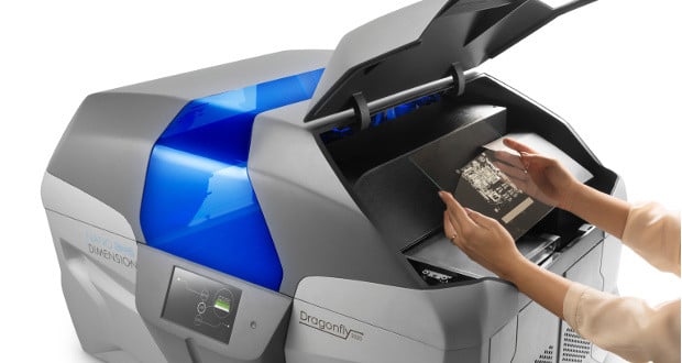
The DragonFly 2020 itself uses the same technology developed by Stratasys’ PolyJet in order to print multilayer circuit boards in a matter of hours. The system produces metal and polymer combination prints, which are ideal for PCB and electronic prototypes. Once printing is complete, auxiliary electronics such as: transistors and resistors, are added so that the user can test out the finished PCB prototype.
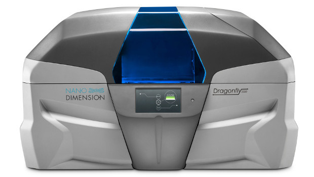
The DragonFly 2020
Using our in-house developed AGCite nanoparticle conductive silver inks and our dielectric inks to create PCBs, our scientists can then use them to produce 10-100 nanometer-sized particles of pure silver. To achieve the best levels of conductivity, flexibility, and adhesion, they can control the size, shape, and dispersion of the nanoparticles.
Our dielectric ink is also unique in that it was engineered to be a functional material with specific properties that are necessary to insulate the conductive ink and allow for the layers of a circuit board to be built. In addition, the dielectric ink features high thermal stability, able to withstand very high temperatures of up to 350° C (662° F).
3DN: What are the benefits of 3D printing when it comes to the production of electronics?
Having the ability to merge printed electronics and 3D printing is bringing more innovation to both worlds. The typical two-week turnaround for a 10-layer PCB can often mean that engineers remain conservative during the design process, as any mistakes can come with high risk in terms of cost and time. With 3D printed electronics, engineers can be more innovative, changing the way the work and having more flexibility during the process. This could have a strong impact on the production of consumer technologies. An example can be with how PCBs are designed, allowing us to soon have the ability to produce coils and even embed electronics.
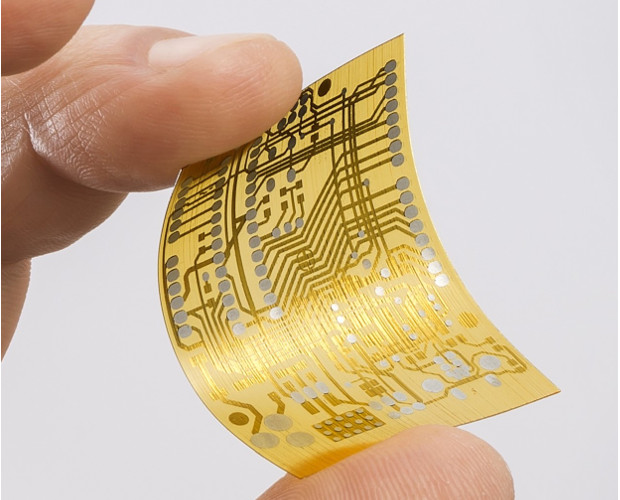
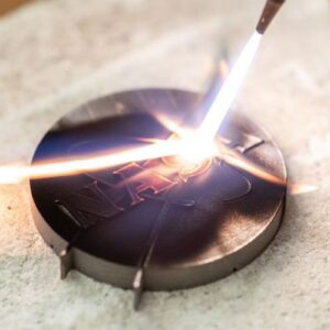
A printed circuit created thanks to additive manufacturing
3DN: How do you envision the future of 3D printed electronics?
The holy grail of 3D printing is to have the ability to print fully functional customized objects in one build, including in complex electronics. This is one of our goals and what we have started to do with the DragonFly 2020. In the future, 3D printed electronics will use a broader range of materials, while having greater flexibility when combining materials. We are also expecting a continued growth in 3D printing systems. With the ability to overcome some of the sector’s problems such as: speed, scale, and precision.
3DN: We heard about your recent launch of a 3D bio-printing subsidiary. Could you tell us a bit more about this?
We believe that by mixing our knowhow in multi-material 3D printing and our expertise in nano-chemistry, that we will be able to provide a significant added value to the promising field of bio-printing, allowing us to create very complex biological structures. We hope to advance this initiative through this subsidiary, by focusing solely on 3D bio-printing. So far, we have demonstrated a successful proof of concept by 3D bio-printing tissue with stem cells. We have also filed a patent application for our bio-printing technology.
3DN: Any last words for our readers?
The DragonFly 2020 is currently being evaluated by beta customers in a variety of industries, including: defense, consumer goods, technology for the finance industry, and medical devices. They system is scheduled for commercial release later this year in key manufacturing and tech areas in the U.S., Europe and Asia.
More information on Nano Dimension’s technology can be found here. Also, check out our interview with Simon Fried at Solidworks World 2017 :
What is the future of 3D printing in the electronics industry? Let us know what you think in a comment below!


Do you have a nanoparticle inkjet printer that can print oxide semiconductor materials with sizes ranging from 100nm to a few micrometers? What are the main performance parameters, and ideally, the price should be around $100,000. My location is in China.