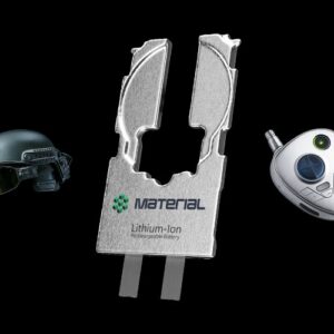
Nano Dimension on the Future of Electronics in Additive Manufacturing
Additive manufacturing has been growing in importance in a number of different industries in the past few years. The ability to create objects that are customizable, more optimized, and often cheaper than parts created through traditional methods has made AM invaluable in a lot of critical sectors. However, there is one industry where AM has been struggling to make its mark: electronics. While sectors like aerospace and automotive have been using AM for years, 3D printing has made less of an impact overall on the electronics industry. That being said, microscale additive manufacturing has been growing exponentially in recent years, with companies working to advance Additive Manufacturing Electronics (AME) technology. One of the leaders of this movement is Nano Dimension, a manufacturer of 3D printed electronics systems that uses their own proprietary inkjet printing technology and nano-inks to create precise electronic parts for a variety of industries including medical, automotive and aerospace. They are also noted for their extensive contributions to pushing research and working with academia to help redefine how we think about AME technologies and what it is possible to create. We spoke with Valentin Storz, the General Manager of EMEA at Nano Dimension, to learn more about their technology, the applications of 3D printed electronics and engaging with academia to push the boundaries of existing technology and help to train the next generation of engineers.
3DN: Can you introduce yourself and your connection to AM?
 My name is Valentin Storz, I am located in Germany and have worked for the past two and half years with Nano Dimension. Before that, I spent six years with Makerbot and Stratasys running the European operations. It was an interesting ride when Stratasys bought Makerbot in 2014. At this time, the whole world of 3D printing looked quite a bit different.
3DN: What about Nano Dimension? How was it started? What is its mission?
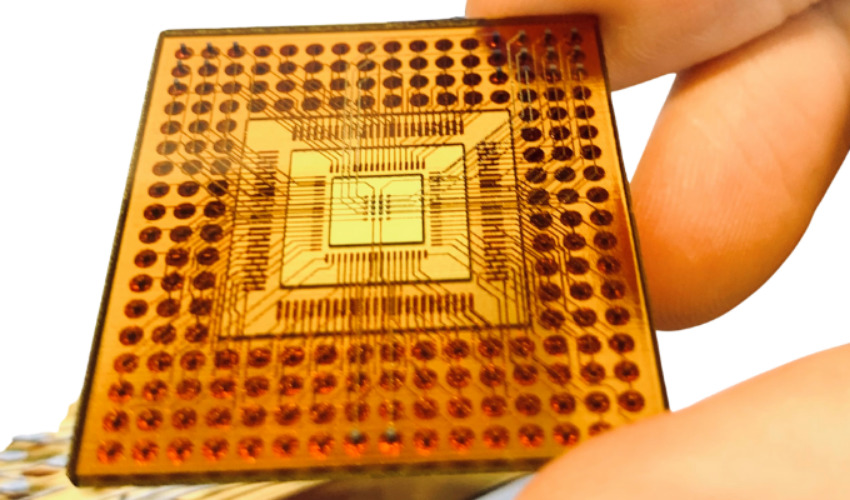
Nano Dimension is the company that is electrifying additive manufacturing. It is the company that has technology that comes in a system the size of two refrigerators, called DragonFly LDM®. The system has the ability to jet simultaneously dielectric and conductive inks to 3D print free form electronic parts. We are bridging the gap between the PCB and Semiconductor Industry with the development of Hi-PEDs™ (High-Performance Electronic Devices). These are more than just circuit boards with printed components; they have coils, capacitors, complex circuitry, transformers and more. We are also involved in a number of projects and industries. For example, we produced a 3D printed Radio Frequency (RF) Amplifier that was sent to the international space station. The mission of Nano Dimension, is to revolutionize electronics AM.
3DN: Can you tell us some more about your Lights-Out Digital Manufacturing technology? What about the DragonFly LDM Manufacturing System?
DragonFly, is equipped with our state-of-the art, proprietary Lights-Out Digital (LDM) Manufacturing technology. LDM allows for unattended operation as it maintains itself, with typically just one weekly maintenance operation needed. Currently, it is the industry’s only comprehensive additive manufacturing for around-the-clock 3D printing of electronic circuitry. This is thanks to improvements in the system like a new advanced printer head, software management algorithms and automatic-self-cleaning of the print heads every few hours. It is a precise inkjet deposition printer with dedicated nano-inks and optimized 3D software for printing electronic circuits, setting new precision standards for 3D printed electronics.
3DN: What are the applications of the technology?
There are a variety of applications for AME. Of course, there are Printed Circuit Boards (PCBs), but it is also particularly useful for advanced RF solutions, things like Omni Antennas, 5G, MEMS, Advanced Sensors, Non-Planar Multi-Layer Electronics, and HDI. You can just input what you need, define the shape, etc. and then it is ready to print. As you can imagine, this has many advantages for RF technology. It can be used as well for packaging solutions, IC shielding or even sensors. Touch sensors are an important application as these sensors have applications for devices in the medical, industrial, and automotive fields. That being said, it is a relatively young technology in the AM word. What we are seeing mostly at the moment is how it is being used for research purposes. For these reasons, we are focusing on enabling researchers and academics as we see publications in the field growing rapidly. The research and academia sectors are looking more and more into this technology.
3DN: What would you say are the next steps in 3D printing technology? How do you think the AM electronics market will evolve over the next few years?
In the next few years, I think we will see the growing influence from research academia, defense, medical, and other specialized solutions. When you look at PCB, that’s a 7-billion-dollar market, and it’s just at the top of this industry pyramid. There is still the part of the industry that is even more specialized. There will be new form factors, miniaturization, integration of assembly steps and components and ultimately, digital inventory which will then allow for further development of electronics in AM.
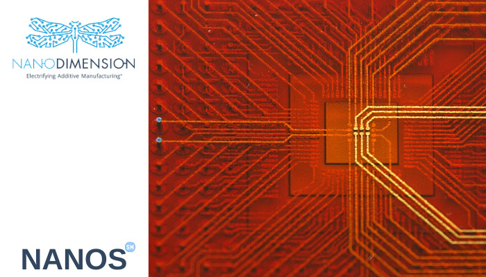
Nano Dimension also has a 3D printing service, NaNoS (photo credits: Nano Dimension)
3DN: What is the importance especially of the role of academia when it comes to electronics design and teaching the next generation of engineers?
Education is crucial in the additive manufacturing field, and especially when we are talking about AME. As it is right now, no one is learning how to design for that type of technology. As a direct result of that, many people will only think in the bounds of traditional technology. But with AME, the industry is dealing with very new machines that require a new approach on design development and understanding of materials and systems. With traditional methods you are limited in what you can do because it’s not really 3D. The new generation of engineers are coming out and they are pushing for 3D electronics. They are looking into the opportunities from it and they are coming up with new ideas.
We have made it a mission to work with universities and the wider industry and look into programs to advance these educational programs. But speaking frankly, we all need to do a lot more. We can offer not only the machine, which costs about 500,000 dollars, but also the service, NaNoS℠, where students and professors, can use our technology to test and see if what they want to create is possible with 3D printing technology. NaNoS℠ is a cooperative design and fabrication service for anyone who wants to explore the future of AME fabrication. ™It allows professionals to experiment by designing and creating Hi-PEDs™ and test print them on a variety of substrates such as FR4, Silicon, Copper foil and others. We don’t know what will be successful, what research will come out, but we want to try and help advance it where we can.
3DN: Any last words for our readers?
I believe that the impact that AM will have will be much bigger on electronics than even on the mechanical world. You can find more information about Nano Dimension on our website or in the video below.
What do you think of Nano Dimension and AME? Let us know in a comment below or on our Linkedin, Facebook and Twitter pages! Sign up for our free weekly Newsletter here, the latest 3D printing news straight to your inbox! You can also find all our videos on our YouTube channel.
Thumbnail Photo Credits: Nano Dimension