


Additive manufacturing in aerospace is growing

Research and Markets recently published a study of the additive manufacturing market applied to the aerospace sector; the consulting firm announces a growth rate of 23.01% between 2017 and 2021. A forecast that shows the full potential of 3D technologies in the aerospace sector as well as many other possible applications today.
Additive manufacturing in aerospace have been happening for some time now with many applications. Covering everything from the creation of aircraft or helicopter parts, making lighter and more efficient engines, 3D printed turbines etc. 3D technologies generally save on time, money and create stronger, more efficient finished products. The Research and Markets study confirms this idea. In terms of additive manufacturing disrupting aerospace and it being widely praised by many players as they announce the possible growth rate of 23.01% between 2017 and 2021.
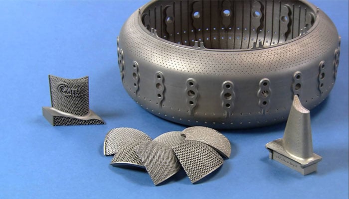
3D printed parts by EOS for MTU Aero Engines
The aerospace sector should combine additive manufacturing and traditional methods
The report have been produced with the help of several industry experts. It covers the entire market and its growth prospects over the next few years. One of the trends revealed by this report indicates that the market should increasingly combine additive manufacturing and traditional manufacturing. 3D printing would be more involved in the product development phase by providing the ability to create functional prototypes or molds in a faster and more cost effective manner.
According to the report, the aerospace sector would mainly use additive manufacturing to improve the performance of a part and reduce its weight. 3D technologies would offer more freedom in the design of parts that can be more complex while remaining efficient. They would also facilitate the integration of parts, removing some design and production constraints.
Current challenges with additive manufacturing in aerospace
The report goes on to explain that one of the challenges of the market is the restriction of the volume of construction and the size of the product. An aircraft is made up of very large components and additive manufacturing is today limited to the volume offered by the 3D printer. Most technologies offer solutions with limited print volume, making 3D printing applicable only to small components. So we still have this constraint that could slow down the growth of the market. Even if so today’s 3D technologies have already made it possible to create fairly large pieces. An example is the fuselage panel created by STELIA Aerospace. As well as companies such as GE, that’s already working on expanding the size restraints step by step
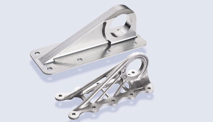
Parts for Airbus, 3D printed by GE
Finally, the report provides an overview of the main players in the aerospace market. These includes Arcam, Arconic, EOS, GKN and Stratasys. Other companies like 3D Systems or Concept Laser are increasingly interested in aerospace additive manufacturing and may well become experts in the industry. Find the whole of the study on the official website of Research and Markets.
Can manufacturing revolutionise the aerospace industry? Let us know what you think in a comment below or on our Facebook and Twitter pages! Don’t forget to sign up for our free weekly Newsletter, with all the latest news in 3D printing delivered straight to your inbox!
The future for Additive Manufacturing is the combination Plasma and High Power Electron Beam, a new system called High Power Plasma Electron Beam Installations (HPPEBI). This new pending patent, HPPEBI designed for applications in additive manufacturing, offers transformative improvements over conventional thermionic electron guns and lasers. The system generates a plasma and high-energy monoenergetic electron beams with any distribution in time and space. The electron beam focus could be cylindrical, circular, rectangular, linear and pinpoint. It is .Important to mention that these multiple focus geometries and tailored heating profiles are determined only by configurable cathodes . Thin or broad electron beams, converging or diverging, can be designed over a wide range of current and voltage. These electron beams transfer energy directly to target materials with a high efficiency (minimum 80%), enabling localized heating, melting, or evaporation with minimal distortion or residual stress..
In different industrial applications, the performance and longevity of materials rely heavily on the accuracy and effectiveness of their surface treatment processes. The involvement of new technologies for the manufacturing of materials, as well as for modification of their structure and properties is of major importance. Many existing patents focus either on electron beam treatment or plasma treatment independently.. My invention uniquely combines both technologies, allowing for more precise control over the heat treatment process, enhancing surface properties and reducing defects. The combined effect of electron beam and plasma can significantly enhance surface properties such as hardness, wear resistance, corrosion resistance, reduce energy consumption, processing time and minimize residual stresses. This dual approach allows for a more controlled modification of the microstructure, leading to superior performance of treated components. HPPEBI exceeds the actual technologies, Thermionic Electron Gun (TEG) and Laser in the following key aspects:
1.Energy Density: the electron energy density is higher in HPPEBI than in TEG or Laser due to several key differences in their mechanisms and operating principles.
HPPEBI: electrons are emitted by a Cathode , which could have any configuration and dimensions. Electron energy doesn’t have any limits. It is determined by the applied voltage.
TEG : electrons are generated by a filament cathode, with small dimensions. The max electron energy is limited by the thermionics emission law of the filament.
Laser:. is working with photons which can have a limited max energy determined by the wavelength and laser power.
2. Energetic distribution of electrons
HPPEBI: Uniform energy distribution. Electrons emitted by the cathode are accelerated in the plasma electric field. This controlled acceleration results in a narrow energy distribution for the electrons, as they all gain energy primarily from the same electric field.
TEG: electrons are emitted from a heated filament cathode due to thermal excitation, which follows the Maxwell-Boltzmann law. The energy distribution is a broad distribution with a Maximum. As a result, TEG produces a wide electron energy distribution with a maximum in a center.
3.Penetration deep in the target.:
HPPEBI: Deep penetration with depth at least 100 µm.. Uniform volumetric heating and melting
TEG: Shallow (surface) interaction. Depth=0.1-10 µm.
Laser: Shallow (surface) interaction. Depth=0.1-10 µm.
4.Operating Temperature
HPPEBI: Can handle higher energy densities for materials with higher melting points.
TEG: Limited by filament temperature tolerance.
Laser : Limited by the laser power.
5. Melting Efficiency
HPPEBI :deliver 80-95% kinetic energy in target directly.
TEG: Around 70%.
Laser: 10-50%..Reflection losses are High (up to 90% in certain metals).
6.Interface (In-Situ) Engineering Capability
HPPEBI: Yes — electrons clean, activate, and bond layers.
TEG: No. Needs pre/post treatment.
Laser: No. Require separate process.
7.Residual Stresses and Interlayer Bonding
HPPEBI: Deeper penetration and stronger bonding minimize residual stress and distortion in components. Also, by controlling the thermal profile and by inducing phase transformations, HPPEBI treatments can significantly reduce the internal stresses that otherwise might compromise the material’s structural integrity. Volumetric melting ensures uniform thermal distribution and elimination of oxidation and gas entrapment.
TEG: Introduce residual stresses and distortion due to localized heating. Weaker interlayer bonding because of partial fusion.
Laser: Surface-limited heating leads to residual stress and weak bonding. Susceptibility to oxidation and porosity due to inert gas environments
8.Processing time
HPPEBI: Production cycle is very short . Because the cathode could have the same area as the powder bed , and the energy density is higher the melting of the entire powder layer can be done in one-shot..
TEG: Slower because the total powder bed area needs multiple scans of the electron beam or laser beam.
9. Thermal Distortion, Thermal Stress and cracking
HPPEBI: The high precision and uniform heating minimize thermal gradients, thermal distortion, reducing the risk of thermal stress and cracking in the treated materials. This is critical for components requiring tight tolerances.
TEG+ Laser: : have broader heating zones which can cause more thermal distortion, making it less ideal for precision applications.
In HPPEBI, Plasma assures a heat treatment of layers before and after the melting.
This innovation HPPEBI offers unparalleled precision, energy efficiency, and reduced operational costs, making it far superior compared with conventional methods like Thermionic Electron Gun and Lasers. Licensing this patent could position USA as a leader in cutting-edge industrial solutions, opening new revenue streams and creating high-tech jobs. By integrating energy-efficient operations and minimizing environmental impact, the system enhances industrial productivity while contributing to sustainable development.
Dr. Elena Avram
Ph.D. in Physics | Research Physicist | Inventor
📧 av*****@***il.com
📞 +1 (443) 694-4622
🔗 [LinkedIn Profile]
.