HENSOLDT and Nano Dimension create 10-layer 3D printed circuit board
Sensor solutions provider HENSOLDT together with the one of the leading Additively Manufactured Electronics (AME) providers, Nano Dimension, has achieved a major breakthrough on its way to utilizing 3D printing in the development process of high-performance electronics components. As you may know, the electronics industry is one of the least well versed in additive manufacturing. Over the last few years, the sector has been slowly integrating AM technologies into its activities for prototyping and small series production. Additive manufacturing can bring new capabilities by enabling a new-level of customization for micro and nanoscale electronics components. Clearly demonstrated by HENSOLDT and Nano Dimension’s new breakthrough.
In fact, utilizing a newly developed dielectric polymer ink and conductive ink from Nano Dimension, HENSOLDT succeeded in assembling the world-wide first 10-layer 3D printed circuit board (PCB) which carries high-performance electronic structures soldered to both outer sides. Until now, 3D printed boards could not bear the soldering process necessary for a two-sided population of components. This application could be useful for many sectors that require a high level of precision and performance. Thomas Müller, HENSOLDT CEO, explains: “Military sensor solutions require performance and reliability levels far above those of commercial components. To have high-density components quickly available with reduced effort by means of 3D printing gives us a competitive edge in the development process of such high-end electronic systems.”
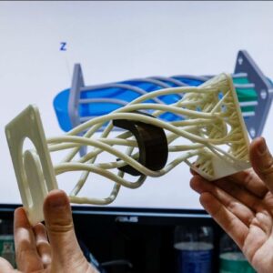
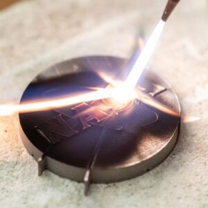
Nano Dimension’s technology can produce 3D printed circuit boards | Credits: Nano Dimesion
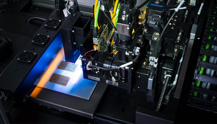
Nano Dimension has developed and been using an inkjet 3D printing technology to produce electronic components for some years now. Based on photopolymerization, their printhead deposits dielectric nanoparticles, conductive nanoparticles and polymers onto the build plate, which are cured by UV light in between successive depositions – creating structures that are conductive and insulating at the same time.
One of the benefits of using 3D printing is shorter time to market compared to creating these components using traditional methods. Also, the cost is reduced for prototypes and small series production, meaning that companies can affordably test designs before implementing. Therefore, AMEs are useful to verify a new design and functionality of specialized electronic components before production, leading to significant reduction of time and cost in the development process.
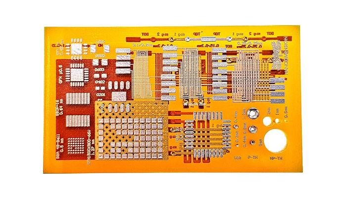
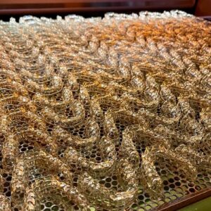
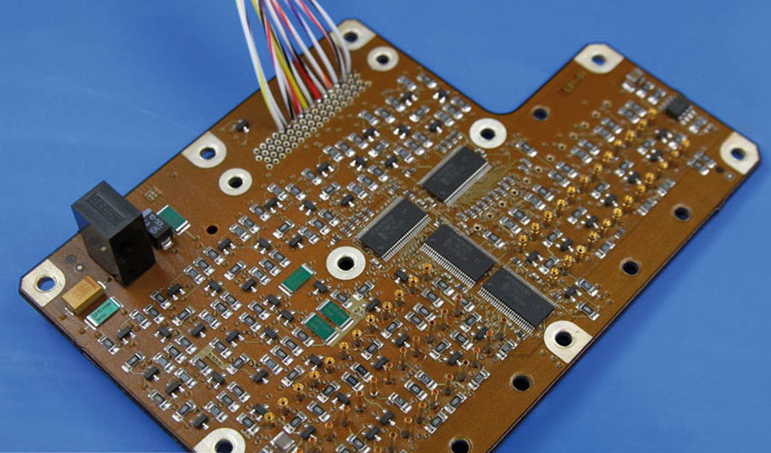
There is a great demand for printed circuit boards (PCBs) to become denser and more complex. The following PCB is multi-layer which means it contains multiple layers of conductive traces instead of containing only 1 | Credits: Nano Dimension
HENSOLDT explains that it actually started working with Nano Dimension’s DragonFly 3D printing system in 2016, in order to examine the possibilities of 3D printing electronics. Last year, HENSOLDT successfully implemented the DragonFly Lights-Out Digital Manufacturing (LDM) printing technology, the industry’s only additive manufacturing platform for round-the-clock 3D printing of electronic circuitry. Yoav Stern, Nano Dimension President & CEO concludes: “Working together and learning from HENSOLDT led us to reach a first-of-its-kind in-depth knowledge of polymer materials applications. Additionally, it guided us in the development of Hi-PEDs (High Performance Electronic Device) that create competitive edges by enabling unique implementations with shortest time to market.”
What do you think of this 10-layer 3D printed circuit board? Don’t hesitate to leave your thoughts in the comments below or on our Facebook and Twitter pages! Sign up for our free weekly Newsletter to receive all the latest news in 3D printing straight to your inbox!
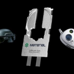
*Cover Image Credits: HENSOLDT